 |
|
Resource Algebra and the Future of FPGA Technology
|
|
|
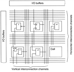
Typical problems of FPGA design FPGAs contain small programmable cells surrounded by programmable interconnections.
The larger the FPGA, the more critical becomes the length of the signal paths. Therefore, interconnections of different lengths (local or global) are provided.
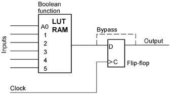
1 - arrays of programmable logic cells; 2 - programmable signal paths; 3 - programmable switching matrices to selectively interconnect different signal paths. The principal structure of a typical cell shows circuitry to implement a Boolean (combinational) function and a flip-flop. One of the most basic requirements to FPGA architecture develoment is that it must be possible to implement arbitrary Boolean functions by appropriately programming cells and interconnections. The application-specific Boolean functions are to be mapped onto those Boolean functions that can be programmed into the cells and interconnections. With regard to complexity, this is a hard problem of Boolean computation. To alleviate the functional decomposition, it is expedient to provide cells, which can implement every desired function of some variables. An obvious solution is to simply store the truth table. Hence the cells of many contemporary FPGA architectures contain lookup tables (LUTs), which are essentially small RAMs or multiplexers, whose data inputs are connected to programmable latches.
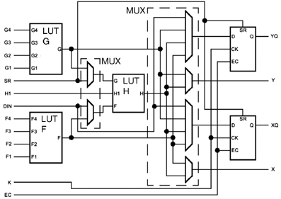
A typical cell accommodates one to four functions, and a similar number of flip-flops. Development software maps arbitrary logical designs onto such cell arrays. The so-called Configurable Logic Block (CLB) is the basic cell of a prevalent FPGA family. It contains three lookup tables (LUTs) and two flip-flops. The multiplexers are programmable, too, allowing different configurations.
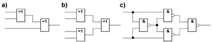
(Source: Xilinx) Cells, transistors, and gates The numbers can be found in advertisements and data sheets. Cells and transistors could be counted, at least in principle. The number of gates, on the other hand, is merely an advertising statement. It is based on the fact that the cells can implement Boolean functions, which would otherwise require a considerable number of NAND gates with two inputs. To obtain a particularly high gate count one can let a cell implement an XOR of all input signals. An XOR of n variables requires n-1 XOR gates with two inputs. Each of them requires four NAND gates with two inputs. In an XOR function, nothing can be minimized. An XOR of 4 variables thus corresponds to 3 XORs with two inputs = 12 NANDs, an XOR of 6 variables corresponds to 5 XORs with two inputs = 20 NANDs and so on. The gate numbers in the manufacturers' data sheets are statistical values similar to processor performance data based on a certain instruction mix.
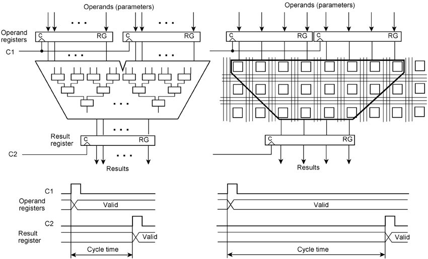
a) XOR of 3 variables; b) XOR of 4 variables; XOR of 2 variables built with NAND gates with two inputs. State-of-the-art FPGAs comprise hundreds of thousands or even millions of gates. So many gates should suffice to implement the most advanced application-specific circuits. The transistor count of large FPGAs is still more impressive. However, the majority of the transistors is used to program the cells and the interconnecting networks. Each bit to program the FPGA has to be stored, requiring typically some kind of latch or SRAM. An FPGA-based implementation will often use up more than ten times the number of transistors when compared to true application-specific circuits, which have been optimized down to the transistor. To mention a historical example, an FPGA comprising 75 million transistors cannot accommodate a processor core comprising 7.5 million transistors. Clock cycles In hard-wired circuits, the gates and switching networks are optimized down to the transistor. The signal paths are kept as short as possible. The clock frequency can be selected as high as the technology permits. In FPGAs, on the other hand, everything has to be built with cells and connected via predetermined signal paths. The clock distribution is also prefabricated. Therefore, circuits in FPGAs cannot be operated at as high clock frequencies as hard-wired circuits implementing the same functions. This figure compares circuits at the register transfer level. The operands are loaded with a clock C1 into operand registers. The results are generated by combinational circuitry. Its delay time determines the minimum cycle time. After the cycle time has elapsed, the results are transferred to a result register with a clock C2. Combinational networks consisting of transistor structures or gates (a) have much shorter delays than functionally similar networks of programmed logic cells (b).
Clock frequencies The processor 1 instruction in frequencies in can operate. 1 among the cells, and so less) interconnections. (high) frequency that the allows. Clock slowdown Ultimately, it is the semiconductor technology that determines the maximum clock frequencies. Compared to circuit solutions, which are optimized up to the transistor, for application circuits in FPGAs a slowdown has to be considered. As a rule of thump, values between 2: 1 and 10: 1 are to be expected. For typical processor-like circuitry, like arithmetic logic units (ALUs), a slowdown in the ratio 10:1 is a useful estimation. The higher the clock frequency in the FPGA, the greater are the design difficulties and risks. One FPGA application clock corresponds to ten processor clocks. A state-of-the-art superscalar processor will execute effectively 2 to 4 instructions in each clock cycle (“effectively” means that valid results are delivered). So one FPGA application clock cycle corresponds to 20 to 40 instructions. In other words, an FPGA solution will be only advantageous, if in one clock cycle, the FPGA can produce results that an innermost loop of 20 to 40 instructions cannot deliver. To alleviate these problems, the manufacturers enrich the FPGAs with optimized, hard-wired blocks, from memory arrays over interface controllers up to fully-fledged superscalar processor cores. Such FPGAs comprise small cells (1) and hard-wired functional units (2), embedded in a grid of programmable interconnections (3). Application-specific circuitry (4) is composed by appropriately programming cells and interconnections.
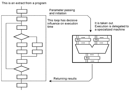
This processors written art allows or even codesign is possible; one requirements are considerable. the beginning, which circuit design. Then in software instead. In principle, it is not really difficult: hardware for the highest speed, if cost is acceptable, software for the lowest cost if one gets along with speed. However, the problems are in the details. The interfaces must be defined. Functional units have to be designed. Program routines that substitute functional units must interact with the remaining circuitry. For that, problems of the program initiation, parameter transfer, synchronization, etc. are to be solved. Communication between programs and functional units can become a difficult development task, especially when the programs have to fit into a given system and runtime environment. Hardware-software codesign (1). The application problem has been solved by writing a program. Performance-critical loops are relegated to special-purpose circuitry.
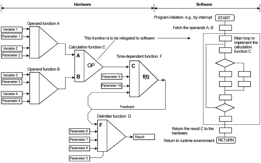
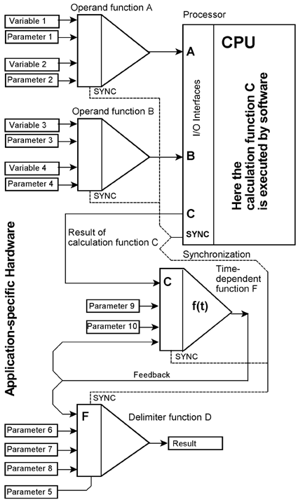
Hardware-software codesign (2). The application problem has been solved by hardware design, here illustrated by a (somwhat sketchy) block diagram. One of the functions (which is rather complicated, but not that performance-critical) is to be relegated to software.
To run the software requires a processor. The application-specific function blocks are to be connected to the processor. The effort depends on the processor's I / O interfaces. Attaching to microcontroller ports is easy, adapting application-specific circuitry to high-performance standard interfaces* is a formidable task in itself. All components have to be synchronized. The software, which emulates the hardware functions must dovetail with the runtime environment of the processor. Sometimes, such programs must run in the supervisory state. Therefore, they must be written as device drivers... *:Like Ethernet, PCI Express, USB 3, or a SoC bus system like Amba, Avalon, CoreConnect,Wishbone, etc.
The vast majority of application developers are programmers, but not hardware designers. Indeed, it is possible to generate automatically hardware designs based on behavioral descriptions, whereby the behavioral description is very similar to a usual program text. Nevertheless, one must know how hardware works and what the development system will generate from certain language constructs. Finally, the compound solution has to be brought up, requiring to locate and troubleshoot problems in both areas (software and hardware). Therefore, it is still a lengthy development process, requiring unique skills and experience. When such systems have been sold, problems may arise how to deploy engineering changes together with software updates. Those problems have stimulated research aimed at synthesizing hardware solutions from conventional program code. The application platform is a pre-punched (so to speak) combination of general-purpose processors and FPGAs, both connected together via predefined, standardized hardware and programming interfaces. The typical philosophy is to support conventional software with dedicated hardware to execute performance-critical functions. Those supplementing devices are essentially acceleration units (accelerators), which the processor addresses with extended machine instructions. When the hardware is implemented with FPGAs, it can be modified over and over. It is tempting to write the solution of the application problem as a program and to leave it to the FPGA development system to synthesize the functions to be relegated to dedicated hardware. Here, however, the intricacies of the circuit synthesis can become noticeable, especially with regard to the depth of the combinational circuitry and the associated clock slowdown. Here, the functions of a program routine have been relegated to an FPGA. The circuitry has been generated by the development system. The combinational networks have a certain depth, thus allowing for a minimum cycle time.
Now, the program has been changed. Therefore, the FPGA circuitry must be synthesized again. However, this can yield deeper combinational networks. Consequently, the cycle time has to be increased accordingly.
|
|
|
|
February 2, 2019 Download an introductory presentation Download two (short) research reports
|
||||||||||||||||
 (Source: Texas Instruments/Actel)
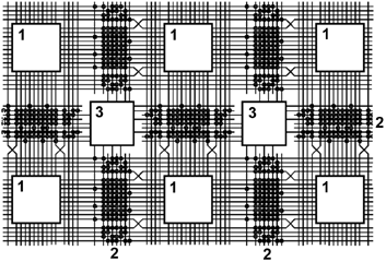 (Source: Xilinx)