|
Level translation with discrete or SSI components
Level translation problems can be solved with discrete or SSI components, such as Zener diodes, bipolar junction transistors (BJTs), field-effect transistors (FETs), and comparators. Zener diodes and MOSFETs are well-suited to translate 24-V to logic signals (down to 3.3 V or below). BJTs and comparators may be employed in both directions.
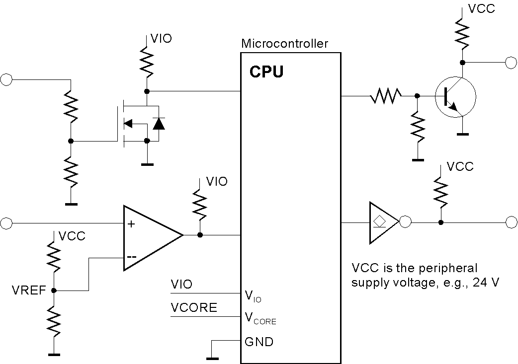
It may be a viable idea not only for tinkering but for high-volume manufacturing too. For instance, think of a household appliance where the microcontroller has to energize four relays and to sense two limit switches. Discrete components are inexpensive. They are not that demanding with regard to PCB design. Often two layers will suffice. Using SMT parts, not that much PCB area will be occupied, and automated manufacturing will keep cost low.
|
Components
|
Minimum input level to switch the output ON
|
Maximum output voltage
|
|
Bipolar Junction Transistors (BJTs)
|
> 0,7 V
|
As VCEmax allows
|
|
FETs
|
A few volts, depending on the maximum permissible RDSON value
|
As VDSmax allows
|
|
Darlingtons
|
> 1,4 V (sum of the VBEsat of both transistors)
|
As VCEmax allows
|
|
Comparators
|
According to the specified input common-mode voltage range
|
As output specification allows
|
|
Optocouplers
|
According to the LED or input specification. Rough estimation: > 1 V above forward voltage (typical > 2.5 V)
|
As output specification allows
|
|
Open-collector or open-drain outputs
|
According to the input specification of the particular component
|
As output specification allows
|
|
CPLDs
|
< 1.2 up to 3.3 V
|
3.3 V or 5 V
|
An IEC 61131-2 compliant input translated using Zener diodes ([37]):
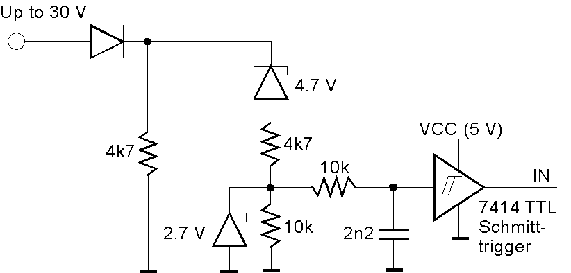
The 4.7-V Zener begins to conduct if the input voltage exceeds approx. 5 V, thus guaranteeing a LOW level as long as the input voltage is less than 5 V. The 2.7-V Zener limits the input voltage of the 7414 Schmitt trigger. The 10k/2n2 combo acts as a low-pass or de-glitching filter.
How to drive a BJT:
The decisive data sheet value is the Base-Emitter Saturation Voltage VBE(sat). Small-signal BJTs are rated typically between 0.7 V and somewhat above 1 V. To keep the transistor safely in the OFF state, the base-to-emitter-voltage should be kept well beyond VBE(sat), say, for example, at approx. 0.3 V. To switch it on, the signal source should deliver a voltage well above 1 V. Then the current path from the base to the emitter will behave like a diode operated in forward direction. Therefore, it is necessary to limit the base current. When no anomalous conditions will occur, especially when the signal source is a CMOS logic output, then the current–limiting resistor alone may suffice. It's value according to a proven rule of thumb:
(Signal voltage – VBE(sat)) divided by a tenth of the output current.
For 24-V inputs, however, you would be better off with the voltage divider, eventually combined with a Zener-based voltage limiter.
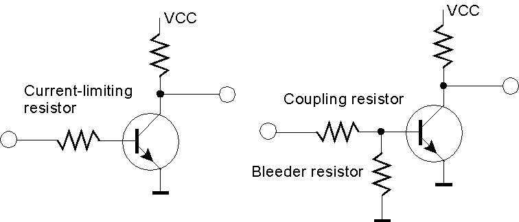
The two most basic circuits. Some manufacturers offer transistors with a built-in current-limiting resistor or coupling/bleeder resistor combo ([38]).
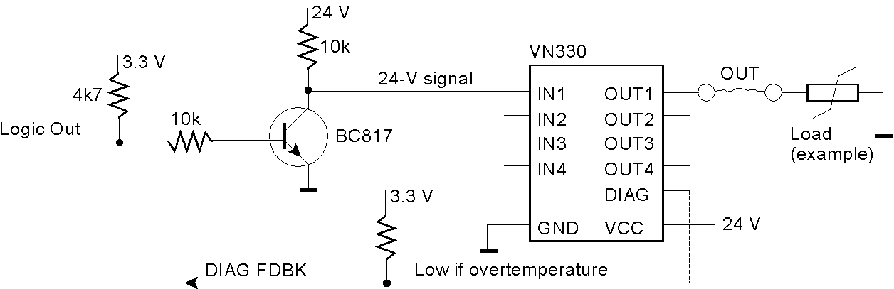
An application circuit translating 3.3-V signals to 24 V ([37]). The pull-up resistor keeps the transistor switched ON when the input is floating. Consequently, the VN330 will not energize the attached load.
The BJT switched ON
The most important data sheet value is the Collector-Emitter Saturation Voltage VCE(sat). Small-signal BJTs have typical data sheet values around 0.2 V. However, to keep the voltage this low, the transistor must be operated in saturation, that is, overdriven by a base current sufficiently high. (Hence we divide the output current by 10 and not by the current-gain parameter h21E or Beta in the data sheet.)
How to drive a MOSFET
In contrast to the BJT, which is controlled by the base current, the MOSFET is controlled by the gate voltage. To keep the transistor safely in the OFF state, the gate-to-source voltage should be kept well below the Gate-Source Threshold Voltage VGS(th). Typical values are between somewhat under 1 V up to somewhat around 5 V. To switch the transistor on, you have to consider the minimum gate voltage that guarantees the data sheet value of the Drain-Source Resistance RDS(on). 10 V is a common value. Observe that the VGS(th) data sheet value relates not to a transistor completely switched ON but to the transitional range between OFF and ON. VGS(th) is often specified as a gate voltage permitting a mere weak drain current to flow (for example, as low as 250 µA).
The most basic circuit:
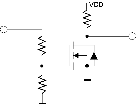
The MOSFET switched ON
FETs are voltage-controlled variable resistors. The voltage drop VDS between drain and source results from the drain current flowing through the drain-to-source resistance (VDS = ID • RDS(on)). So keep the gate voltage high enough and the drain current only as high as necessary.
Level translation with comparators
The comparator is a high-gain, non-feedback differential amplifier. The output should assume only one of two levels (Low or High), depending on the voltage difference VDIFF between the inputs. Many comparator ICs have open-collector or open-drain outputs. The output voltage swing may be as large as the appropriate data sheet parameter permits; it does not depend on the comparator's supply voltage. Thus, for example, a comparator supplied with 24 V may output 3.3-V signals.
The most basic circuit. The comparator's supply voltage VDDin corresponds to the input signal level.
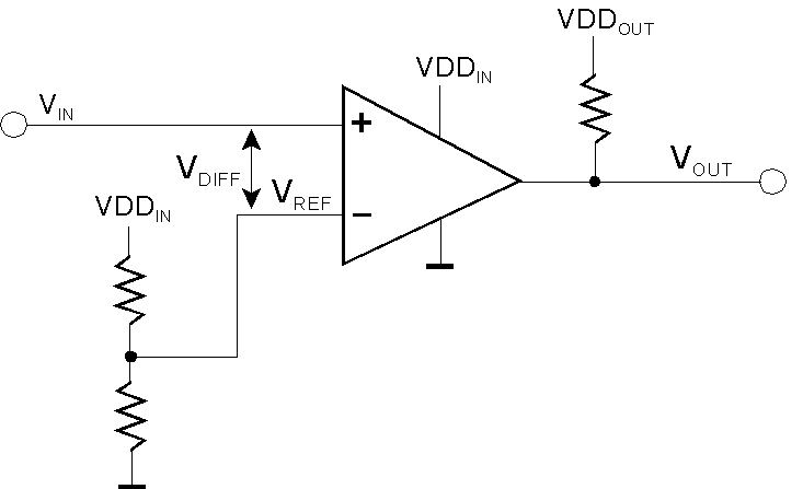
It seems straightforward to employ a comparator. Connect one input to the signal to be translated and the other input to an appropriate reference voltage, which may be provided by a simple voltage divider. There are, however, a few caveats. Here, we will only mention the two most important: the slew rate of the input signal and the input common-mode range.
A comparator has no built-in snap-action mechanism. The threshold effect results solely from the high voltage gain, causing even a small difference in input voltages to overdrive the amplifier. If this difference is very small, however, there will be no overdriving. Parasitic feedback effects could cause the output even to oscillate. On the other hand, if this so-called linear region is traversed fast enough, the comparator will find no opportunity to switch back and forth. Hence only a single signal edge will occur. Thus you have to consider the rise and fall times of the input signal. If they may be too slow, the simple circuit will not work properly. Well-proven remedies you will find in the literature, for example, the Schmitt-trigger circuit or to introduce a particular input behavior, called hysteresis ([39], [40]).
The input common-mode range is typically somewhat smaller (at least some hundreds of millivolts) than the voltage difference between both power supply terminals. This may be a problem if the negative power terminal is connected to the ground (single-ended operation). If the LOW level of your input signal is nearly equal to 0 V (for example, if it is driven by a CMOS logic output switching rail-to-rail), you should prefer a comparator that will function properly in such a case. This property is termed ground sensing in single-ended applications (or something like that).
Watch out for anomalous conditions at the inputs
More intricate problems like ESD, power line interference, crosstalk, and so on we cannot discuss here. They are typical of true factory floor environments. When pursuing humble hobbyist or educational projects, the environment will not be that harsh. There are, however, two conditions you should consider even under those benign circumstances: The first is no signal at all, that is, an open input. The second is a high-impedance (tri-stated) signal. This condition may occur during initialization or as a consequence of faults. A microcontroller running self-tests, communicating via the network, and the like before initializing its output ports may cause such signals to float for a prolonged time. Under both conditions, you should guarantee your translation circuit sees a definite LOW or HIGH input level. Which of both levels to choose as the default depends on the particular application.
MORE ...
|